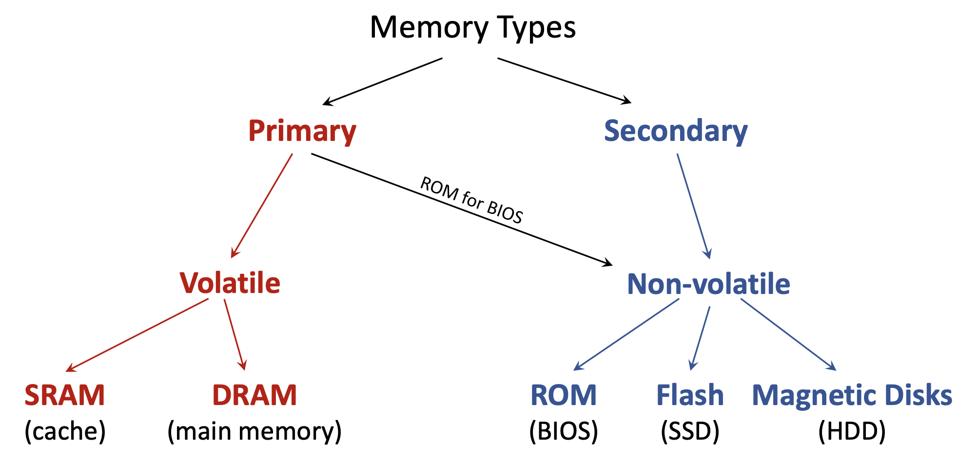
1.8.3 Primary и secondary memory
- Primary Memory — память, с которой CPU работает напрямую; почти всегда volatile (кэш, RAM, ROM с BIOS).
- Secondary Memory — накопители: данные сначала подгружаются в primary; non-volatile.
Hardware Description Language (HDL) — специализированный язык для описания структуры и поведения электронных схем, прежде всего цифровой логики. В отличие от программы, которая исполняется на процессоре, HDL описывает физическое hardware: как соединены вентили и как они должны работать. SystemVerilog — современный мощный HDL для проектирования и верификации цифровых чипов.
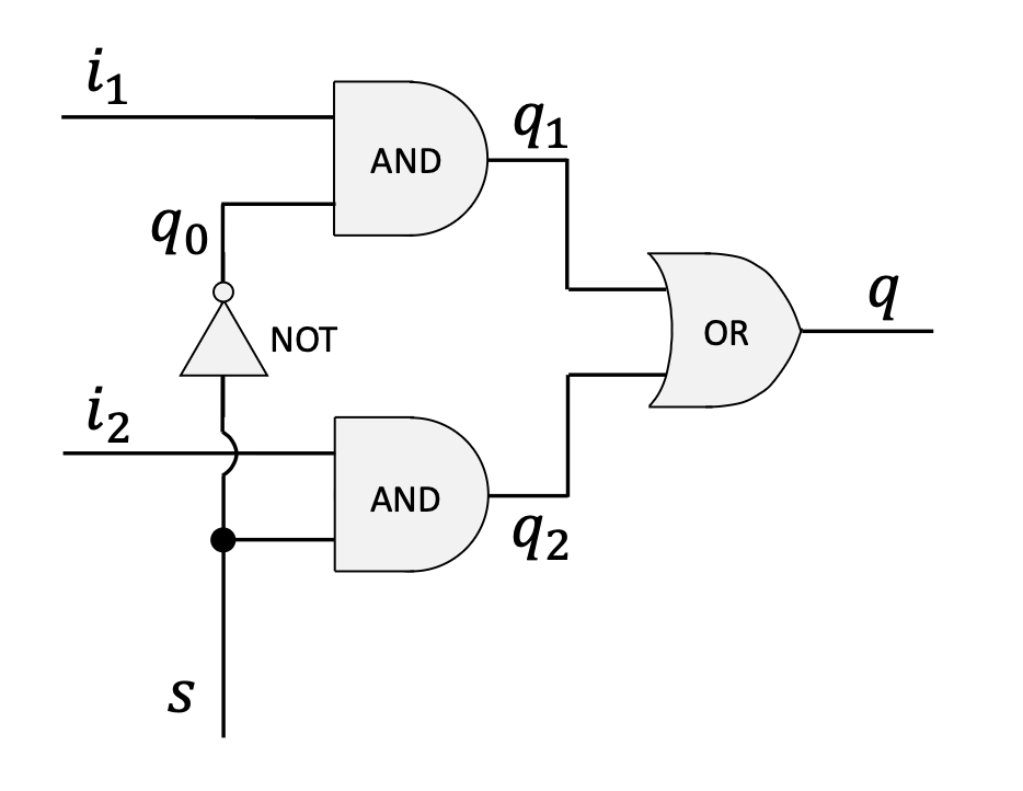
Multiplexer (Mux) — базовая цифровая схема, которая по select lines подключает один из входных сигналов к одному выходу.
У мультиплексора 2-к-1:
i1 и i2;s;q.Поведение:
s = 0, то q = i1;s = 1, то q = i2.Схему собирают из двух AND, одного OR и одного NOT.
Ниже — описание модуля на SystemVerilog.
// 1. Module Definition: Declares a new hardware module named 'mux'.
//    The parentheses list all external connection points (pins):
//    three inputs (i1, i2, s) and one output (q).
module mux (i1, i2, s, q);

  // 2. Pin Direction Declaration: Specifies which pins are inputs
  //    and which are outputs.
  input  i1, i2, s;
  output q;

  // 3. Internal Wires: Declares internal wires to connect the
  //    logic gates. These are not visible from outside the module.
  wire q0, q1, q2;

  // 4. Gate Instantiation: Describes the logic gates and their
  //    connections. For Verilog primitives, the output pin is
  //    always listed first.

  // A NOT gate to invert the select signal 's'. Output is 'q0'.
  not(q0, s);

  // An AND gate combining input 'i1' and the inverted select 'q0'.
  // Output is 'q1'.
  and(q1, i1, q0);

  // An AND gate combining input 'i2' and the original select 's'.
  // Output is 'q2'.
  and(q2, i2, s);

  // An OR gate to combine the outputs of the two AND gates.
  // The final result is the module's output 'q'.
  or(q, q1, q2);

// 5. End of Module Definition
endmoduleВ SystemVerilog можно компактно задать направление прямо в списке портов — семантически эквивалентно предыдущему варианту.
module mux (
  input  i1,
  input  i2,
  input  s,
  output q
);
  // ... module logic ...
endmoduleВместо примитивных вентилей логику часто задают операторами «как в языке программирования»:
~: побитовое NOT&: побитовое AND|: побитовое OR^: побитовое XOR?:: тернарный операторassignКлючевое слово assign задаёт continuous assignment: прямую комбинационную связь правой части с выходом слева. При любом изменении входов справа выражение немедленно пересчитывается — удобный способ описать combinational logic без состояния.
Например, and(q1, i1, q0); можно переписать так:
assign q1 = i1 & q0;Это описывает поведение без явного именования вентиля.
С помощью assign MUX записывают короче.
module mux (i1, i2, s, q);
  input  i1, i2, s;
  output q;
  wire   q0, q1, q2;

  assign q0 = ~s;
  assign q1 = i1 & q0;
  assign q2 = i2 & s;
  assign q  = q1 | q2;
endmodulemodule mux (i1, i2, s, q);
input i1, i2, s;
output q;
assign q = (i1 & ~s) | (i2 & s);
endmodulealways_combalways_combProcedural block — ещё один стиль описания. always_comb предназначен для комбинационной логики: синтезатор ожидает, что блок «срабатывает» при изменении любого релевантного входного сигнала.
always должны быть переменного типа, например logic; выход задают как output logic q;.begin и end.module mux (i1, i2, s, q);
input i1, i2, s;
output logic q; // 'q' must be a variable type
always_comb
begin
q = (i1 & ~s) | (i2 & s);
end
endmoduleВнутри always_comb используют blocking assignments с оператором = — строки исполняются последовательно; следующая не начнётся, пока не завершится текущая. Это стандарт для моделирования комбинационной логики.
always_combПроцедурные блоки позволяют писать более абстрактно — через if/case.
if-elseПоведение MUX естественно записать через if-else:
always_comb
begin
  if (s == 0)
    q = i1;
  else
    q = i2;
endcasecase часто удобнее при большем числе ветвей:
always_comb
begin
  case (s)
    0: q = i1;
    1: q = i2;
  endcase
endВ чисто комбинационном always_comb нужно определить выход при всех возможных комбинациях входов. Если ветка не покрыта (например, if без else), синтезатор может вывести latch — элемент памяти, удерживающий предыдущее значение. Для комбинационной логики это обычно ошибка: дописывайте else и ветку default в case.
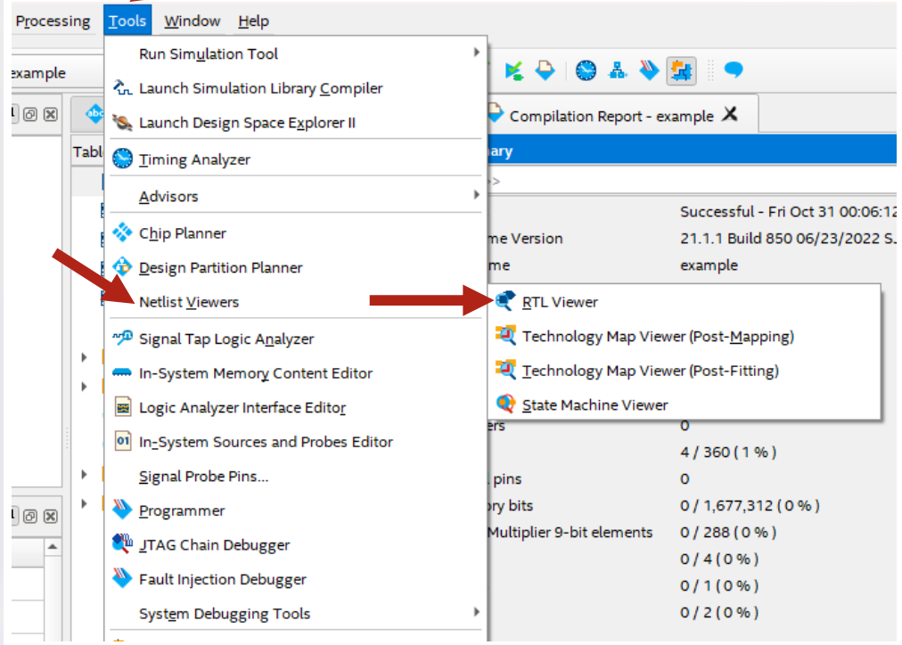
В Intel Quartus Prime есть RTL (Register-Transfer Level) Viewer — по SystemVerilog строится схема синтезированного hardware. Это помогает убедиться, что схема соответствует замыслу. Для MUX 2-к-1 итоговая логика после примитивов, assign или always_comb должна быть эквивалентна.
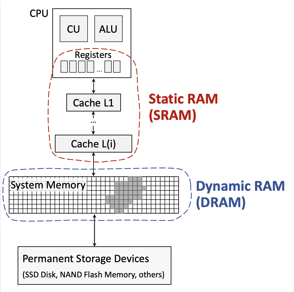
Система балансирует скорость, стоимость и объём: чем ближе память к CPU, тем она быстрее и дороже за байт, но меньше по объёму.
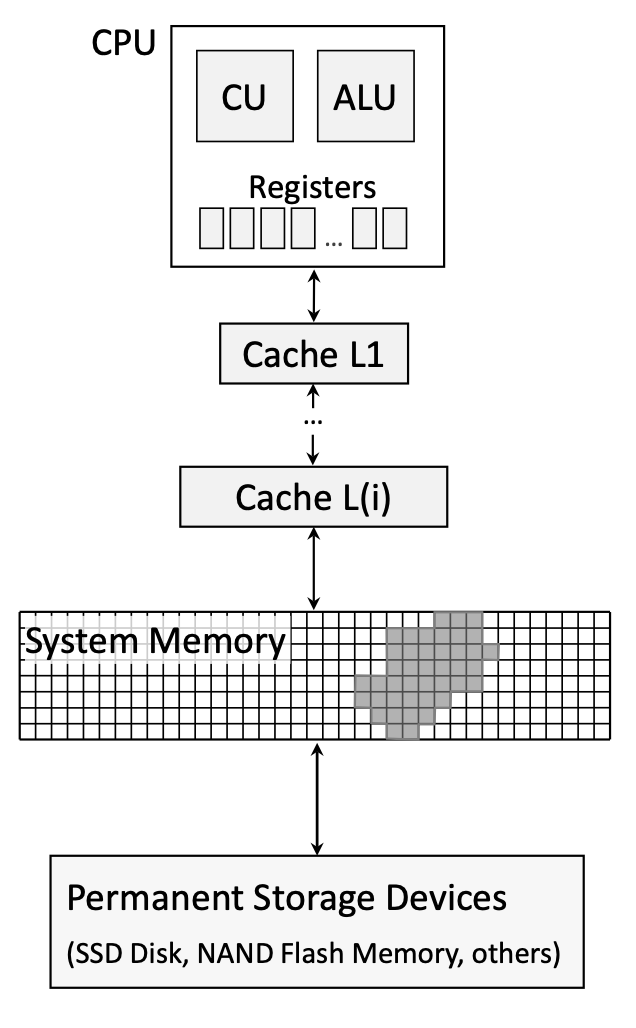
Типичная иерархия:
Иерархия эффективна из‑за locality:
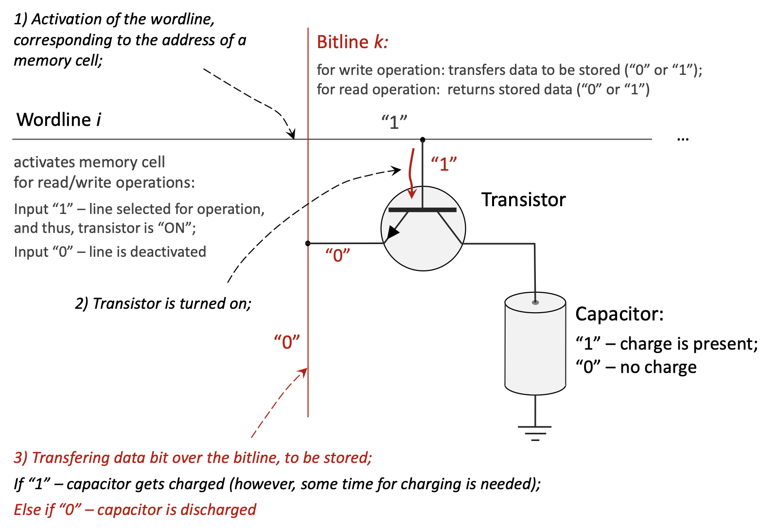
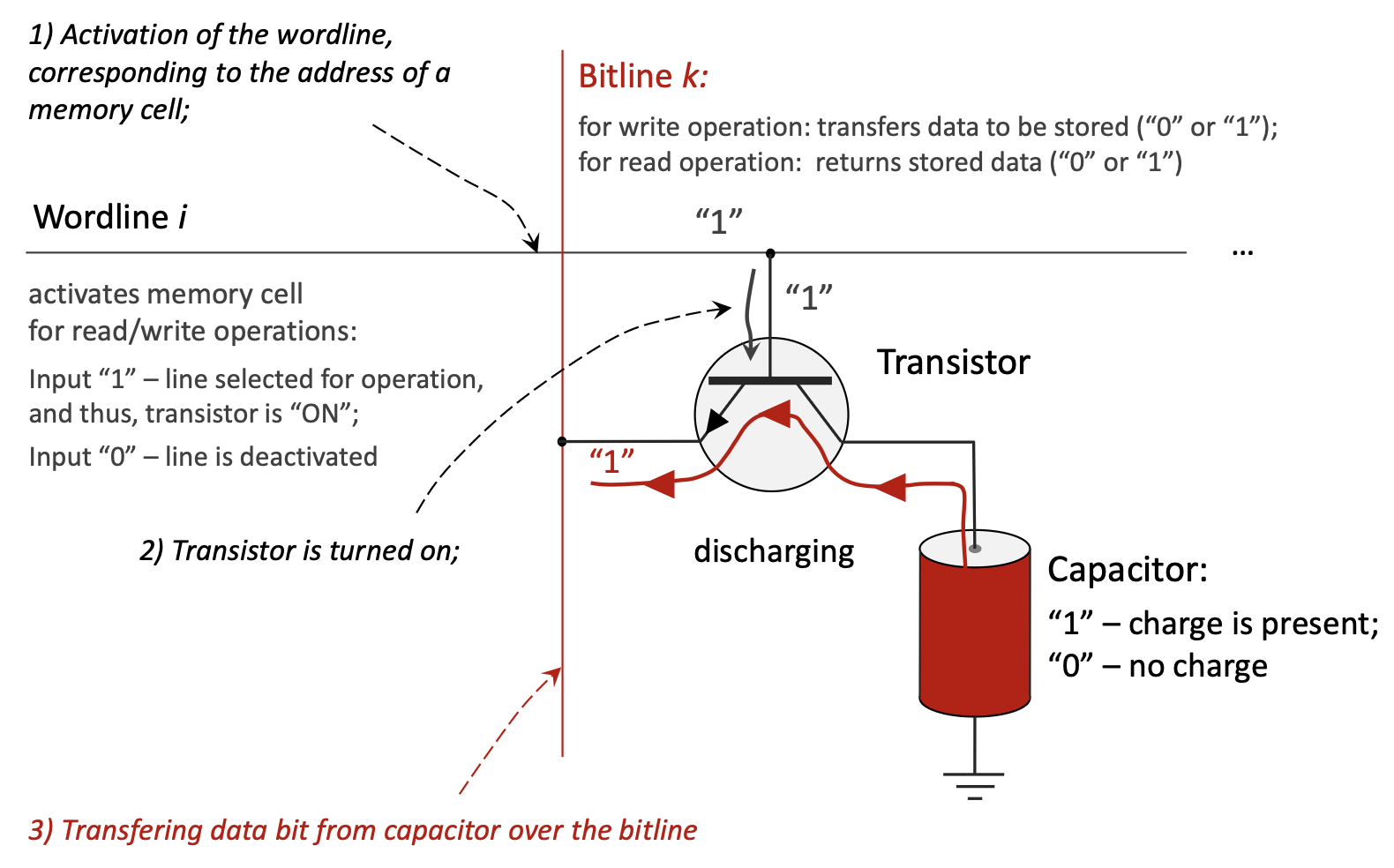
DRAM — основная технология main memory в большинстве ПК. «Dynamic» означает необходимость refresh — периодического восстановления заряда.
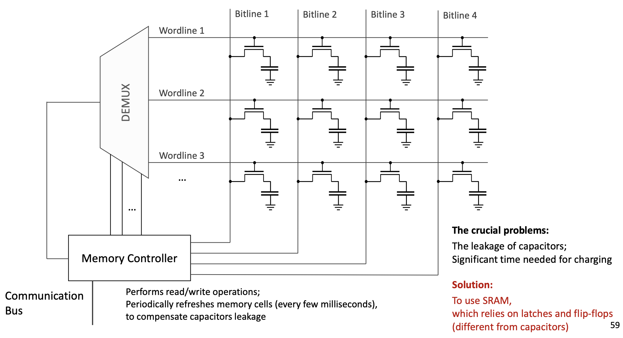
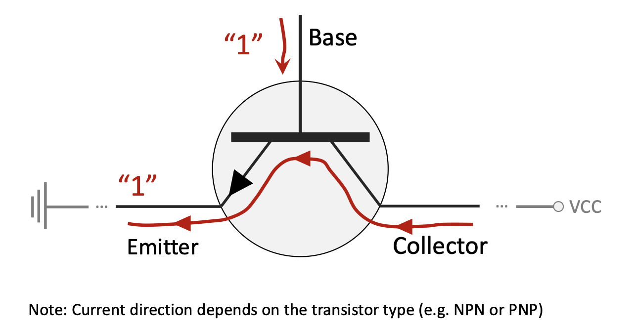
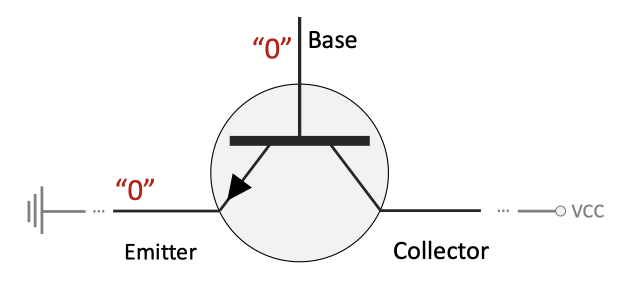
Один бит — это transistor + capacitor:
Ячейки DRAM выстроены в решётку.
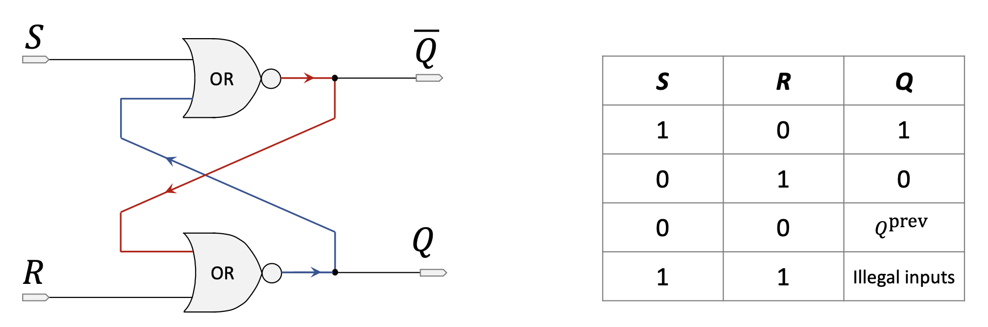
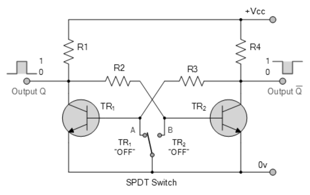
SRAM — технология кэшей и регистров; «static» — без refresh, пока есть питание.
Без отдельного конденсатора как в DRAM: latch / flip-flop, обычно 4–6 транзисторов; два устойчивых состояния; обратная связь удерживает бит.
| Характеристика | SRAM (Static RAM) | DRAM (Dynamic RAM) |
|---|---|---|
| Элемент хранения | Flip-flop (4–6 транзисторов) | Конденсатор + транзистор (по одному) |
| Скорость доступа | Существенно быстрее (порядка 1–10 нс) | Медленнее (порядка 50–100 нс) |
| Стоимость за байт | Дороже | Дешевле |
| Плотность / объём | Ниже плотность, меньше ёмкость | Выше плотность, больше ёмкость |
| Организация | Более сложная ячейка | Проще |
| Утечки / refresh | Пренебрежимо; refresh не нужен | Существенно; постоянные циклы refresh |
| Потребление | Ниже в простое | Выше из‑за refresh |
| Надёжность | Выше | Ниже (чувствительность к soft errors) |
| Volatile | Да | Да |
| Типичное применение | CPU caches, регистры | Main system memory |
assign, модель комбинационной связи входов с выходом.always_comb, описывающий поведение по правилам чувствительности.=): блокирующее присваивание в процедурном блоке.Раздел описывает проект 1-to-4 demultiplexer на процедурном always и testbench для проверки.
// Module: demux_1_to_4
// Description: Implements a 1-to-4 demultiplexer.
// It takes one data input (din), two select lines (sel),
// and routes the input to one of the four output lines (dout).
module demux_1_to_4(
    input din,          // Data input
    input [1:0] sel,    // 2-bit select line
    output reg [3:0] dout // 4-bit data output
);

    // The 'always' block is sensitive to any changes in the inputs (din or sel).
    // This is a combinatorial circuit, so any input change should immediately
    // affect the output.
    always @(din or sel) begin
        // A case statement is used to check the value of the 'sel' input.
        case(sel)
            2'b00: dout = {3'b000, din}; // If sel is 00, route din to dout[0].
            2'b01: dout = {2'b00, din, 1'b0};  // If sel is 01, route din to dout[1].
            2'b10: dout = {1'b0, din, 2'b00};   // If sel is 10, route din to dout[2].
            2'b11: dout = {din, 3'b000}; // If sel is 11, route din to dout[3].
            default: dout = 4'b0000;      // Default case to avoid latches.
        endcase
    end

endmodule

//
// Testbench for the 1-to-4 Demultiplexer
//
// Description: This module is for simulation purposes to test the
// correctness of the demux_1_to_4 design. It is not synthesizable.
// Part c) of the assignment requires testing on an FPGA, but a simulation
// like this is the first step to verify the logic.
module demux_1_to_4_tb;

    // Declare variables to connect to the demultiplexer module.
    reg din_tb;         // Testbench register for data input
    reg [1:0] sel_tb;   // Testbench register for select lines
    wire [3:0] dout_tb; // Testbench wire for data output

    // Instantiate the module under test (UUT).
    demux_1_to_4 uut (
        .din(din_tb),
        .sel(sel_tb),
        .dout(dout_tb)
    );

    // Initial block to define the sequence of test inputs.
    initial begin
        // Display a header for the simulation output.
        $display("Time\t sel\t din\t dout");

        // Test case 1: sel = 00, din = 1
        sel_tb = 2'b00; din_tb = 1; #10;
        $display("%g\t %b\t %b\t %b", $time, sel_tb, din_tb, dout_tb);

        // Test case 2: sel = 01, din = 1
        sel_tb = 2'b01; din_tb = 1; #10;
        $display("%g\t %b\t %b\t %b", $time, sel_tb, din_tb, dout_tb);

        // Test case 3: sel = 10, din = 1
        sel_tb = 2'b10; din_tb = 1; #10;
        $display("%g\t %b\t %b\t %b", $time, sel_tb, din_tb, dout_tb);

        // Test case 4: sel = 11, din = 1
        sel_tb = 2'b11; din_tb = 1; #10;
        $display("%g\t %b\t %b\t %b", $time, sel_tb, din_tb, dout_tb);

        // Test case 5: sel = 01, din = 0 (to show din is passed correctly)
        sel_tb = 2'b01; din_tb = 0; #10;
        $display("%g\t %b\t %b\t %b", $time, sel_tb, din_tb, dout_tb);

        // End the simulation.
        $finish;
    end

endmodule

// Part b) of the assignment, "Make necessary pin assignments in Pin Planner of Quartus Prime",
// is a step performed within the Quartus software GUI. It involves mapping the Verilog
// ports (din, sel, dout) to the physical pins of the FPGA chip. This cannot be done in code.

// Part c), "Upload the design into FPGA and test program correctness", is the physical
// process of programming the FPGA and verifying its operation with hardware,
// for example, by connecting LEDs to the output pins and switches to the input pins.Код Verilog для halfadder, fulladder, верхнего уровня adder4bit и тестбенча.
//
// Part a) Design halfadder module
//
// Description: A half adder adds two single bits (a and b)
// and produces a sum and a carry output.
module halfadder(
    input a, b,         // 1-bit inputs
    output sum, carry   // 1-bit outputs
);
    // Assign sum using XOR operation.
    assign sum = a ^ b;
    // Assign carry using AND operation.
    assign carry = a & b;
endmodule

//
// Part b) Design fulladder module
//
// Description: A full adder adds three single bits (a, b, and cin)
// and produces a sum and a carry output (cout).
// It can be built from two half adders and an OR gate.
module fulladder(
    input a, b, cin,      // 1-bit inputs (cin is carry-in)
    output sum, cout      // 1-bit outputs (cout is carry-out)
);
    // Intermediate wires to connect the half adders.
    wire ha1_sum, ha1_carry, ha2_carry;

    // First half adder to add input 'a' and 'b'.
    halfadder ha1 (
        .a(a),
        .b(b),
        .sum(ha1_sum),
        .carry(ha1_carry)
    );

    // Second half adder to add the sum from the first half adder and the carry-in.
    halfadder ha2 (
        .a(ha1_sum),
        .b(cin),
        .sum(sum), // Final sum output
        .carry(ha2_carry)
    );

    // The final carry-out is the OR of the carries from both half adders.
    assign cout = ha1_carry | ha2_carry;
endmodule

//
// Part c) Design Top-Level-Entity adder4bit
//
// Description: This module implements a 4-bit ripple-carry adder.
// It uses one halfadder for the least significant bit (LSB) and
// three fulladders for the remaining bits.
module adder4bit(
    input [3:0] a, b,  // 4-bit input values
    output [3:0] sum,  // 4-bit sum output
    output cout        // 1-bit final carry-out
);
    // Intermediate wires for the carry between the adders.
    wire c0, c1, c2;

    // LSB Adder (Bit 0): Use a halfadder since there is no initial carry-in.
    halfadder ha (
        .a(a[0]),
        .b(b[0]),
        .sum(sum[0]),
        .carry(c0)
    );

    // Bit 1 Adder: Use a fulladder with the carry from the previous stage.
    fulladder fa1 (
        .a(a[1]),
        .b(b[1]),
        .cin(c0),
        .sum(sum[1]),
        .cout(c1)
    );

    // Bit 2 Adder: Use a fulladder.
    fulladder fa2 (
        .a(a[2]),
        .b(b[2]),
        .cin(c1),
        .sum(sum[2]),
        .cout(c2)
    );

    // MSB Adder (Bit 3): Use a fulladder. The cout from this is the final carry.
    fulladder fa3 (
        .a(a[3]),
        .b(b[3]),
        .cin(c2),
        .sum(sum[3]),
        .cout(cout) // Final carry-out of the 4-bit addition
    );

endmodule

//
// Testbench for the 4-bit Adder
//
// Description: This module tests the adder4bit module by providing
// various input values and displaying the results.
module adder4bit_tb;

    // Declare variables to connect to the 4-bit adder module.
    reg [3:0] a_tb, b_tb;
    wire [3:0] sum_tb;
    wire cout_tb;

    // Instantiate the module under test (UUT).
    adder4bit uut (
        .a(a_tb),
        .b(b_tb),
        .sum(sum_tb),
        .cout(cout_tb)
    );

    // Initial block to define the sequence of test inputs.
    initial begin
        // Display a header for the simulation output.
        $display("Time\t a\t b\t cout\t sum");

        // Test case 1: 3 + 2 = 5
        a_tb = 4'd3; b_tb = 4'd2; #10;
        $display("%g\t %d\t %d\t %b\t %d", $time, a_tb, b_tb, cout_tb, sum_tb);

        // Test case 2: 7 + 1 = 8
        a_tb = 4'd7; b_tb = 4'd1; #10;
        $display("%g\t %d\t %d\t %b\t %d", $time, a_tb, b_tb, cout_tb, sum_tb);

        // Test case 3: 9 + 8 = 17 (results in a carry-out)
        a_tb = 4'd9; b_tb = 4'd8; #10;
        $display("%g\t %d\t %d\t %b\t %d", $time, a_tb, b_tb, cout_tb, sum_tb);

        // Test case 4: 15 + 15 = 30 (maximum values with carry)
        a_tb = 4'b1111; b_tb = 4'b1111; #10;
        $display("%g\t %d\t %d\t %b\t %d", $time, a_tb, b_tb, cout_tb, sum_tb);

        // End the simulation.
        $finish;
    end

endmodule